Hi, me again,
So I'm looking for someone who may have a spare A13 floppy board. I'm looking to hook up a floppy drive to my C24P sometime in the near future so I'm guessing I'll need one of these boards. (Having never seen an A13 board before, it's hard to imagine what the board exactly comprises of, or wether I actually really need one or wether. Maybe I can just take wires right off the J4 connector on the 505B board??)
Anyway, If I can't find one of these cards, another option is Is to try to reverse engineers one. So in that case I'll need to find some detailed photos of the board, parts side, and solder side, so that I can redraw a PCB layout.
Hope someone can help.
Thanks in advance
Philip
WTD: A13 card or detailed pictures/schematics etc.
-
nama
- Posts: 369
- Joined: Wed Mar 30, 2011 9:44 am
- Location: New Zealand
- Contact:
WTD: A13 card or detailed pictures/schematics etc.
2P (1mhz 32k) - 502 + 8k + CEGMON + garbage collector fix BASIC, D&N MEM-CM9 + 24k, 540 (mono) [SOLD]
4PMF (2mhz 24k) - 505, 540, 527, D13 + 5.25" + Gotek
Superboard RevD - CEGMON + 610 board 24k + D13
Spares - 3 x 527, 1 x 505, Backplane
-
dave
- Site Admin
- Posts: 717
- Joined: Tue Sep 09, 2008 5:24 am
Re: WTD: A13 card or detailed pictures/schematics etc.
Hi Philip,
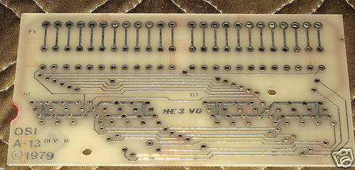
Since my floppy is not currently plugged in to my C2, I was able to scan the A13 board for you. Also, you can check out the bare-board image on Mark's web site
The A13 board looks pretty much like the home-made floppy connector you got with your unit, except that the cables are terminated with the 34-pin edge-card connectors for the shugart standard 5.25" floppy drives. If you have to make an adapter board, I'd suggest plunking down a couple of the 12-pin molex connectors to match your 505 card, and a couple of 34-pin headers to match the standard drive pinout, then match pins and route. That would probably be easier than trying to follow the scans. While you are at it, you could probably throw a data separator right onto the board, and not have to wire one up separately. I was planning on doing the same thing myself, since my OSI floppy needs repair or replacement, but will have to wait until my current project is off to the fab house. Of course, if you do it first, that would be awesome.
Best regards,
Dave
- Attachments
-
- A13-3.jpg (119.87 KiB) Viewed 12131 times
-
- A13-2.jpg (146.07 KiB) Viewed 12131 times
-
- A13-1.jpg (154.41 KiB) Viewed 12131 times
-
nama
- Posts: 369
- Joined: Wed Mar 30, 2011 9:44 am
- Location: New Zealand
- Contact:
Re: WTD: A13 card or detailed pictures/schematics etc.
Thanks Dave...yet again you ROCK!
As I have no skill in any PCB layout software like CadSoft Eagle, I have drawn it by hand using Adobe Illustrator. Basically it's a fairly accurate copy of the original, however I agree with you, if we were going to make a small batch then it would be a great idea to include the data separator circuit, and maybe a switch to turn the separator circuit on and off so that it could still be used with original OSI MPI drives. I also agree that using 34pin headers is also a great solution. The problem is that as I am using Adobe Illustrator, then adding both these things will probably be very tedious work, if I could even do it at all.

Maybe I should take a crash course in using eagle PCB software. I mean...how difficult can it be (famous last words).
As I have no skill in any PCB layout software like CadSoft Eagle, I have drawn it by hand using Adobe Illustrator. Basically it's a fairly accurate copy of the original, however I agree with you, if we were going to make a small batch then it would be a great idea to include the data separator circuit, and maybe a switch to turn the separator circuit on and off so that it could still be used with original OSI MPI drives. I also agree that using 34pin headers is also a great solution. The problem is that as I am using Adobe Illustrator, then adding both these things will probably be very tedious work, if I could even do it at all.
- A-13.jpg (104.68 KiB) Viewed 11966 times
Maybe I should take a crash course in using eagle PCB software. I mean...how difficult can it be (famous last words).
Last edited by nama on Sat Jan 07, 2012 2:38 pm, edited 1 time in total.
2P (1mhz 32k) - 502 + 8k + CEGMON + garbage collector fix BASIC, D&N MEM-CM9 + 24k, 540 (mono) [SOLD]
4PMF (2mhz 24k) - 505, 540, 527, D13 + 5.25" + Gotek
Superboard RevD - CEGMON + 610 board 24k + D13
Spares - 3 x 527, 1 x 505, Backplane
-
Steve Gray
- Posts: 325
- Joined: Mon Oct 06, 2008 1:54 pm
- Location: Markham, Ontario, Canada
- Contact:
Re: WTD: A13 card or detailed pictures/schematics etc.
I'm in the same boat... I recently bought a 505 board with no a13 board. I could use a couple boards with data sep circuit and standard connector. I do have some basic eagle cad skills so I could help out if needed.
Steve
Steve
C4P working, C1P working. 600D Replica working, C4P+D&N floppy not working. 505 board, 610 board, Mittendorf board, TOSIE hacker board need testing, PicoDOS disk untested.
-
nama
- Posts: 369
- Joined: Wed Mar 30, 2011 9:44 am
- Location: New Zealand
- Contact:
Re: WTD: A13 card or detailed pictures/schematics etc.
Hi Steve,
If I could draw up a rough (very rough hand drawn) schematic will all the right connections, switches and jumpers, would you be able to transfer this to Eagle and layout a board design that we could get fabricated?
Unfortunately thats all I can offer considering my lack of PCB layout skill.
Phil
If I could draw up a rough (very rough hand drawn) schematic will all the right connections, switches and jumpers, would you be able to transfer this to Eagle and layout a board design that we could get fabricated?
Unfortunately thats all I can offer considering my lack of PCB layout skill.
Phil
2P (1mhz 32k) - 502 + 8k + CEGMON + garbage collector fix BASIC, D&N MEM-CM9 + 24k, 540 (mono) [SOLD]
4PMF (2mhz 24k) - 505, 540, 527, D13 + 5.25" + Gotek
Superboard RevD - CEGMON + 610 board 24k + D13
Spares - 3 x 527, 1 x 505, Backplane
-
Steve Gray
- Posts: 325
- Joined: Mon Oct 06, 2008 1:54 pm
- Location: Markham, Ontario, Canada
- Contact:
Re: WTD: A13 card or detailed pictures/schematics etc.
Sure, I'm willing to give it a shot. I've been reading the PEEK65 articles and it would be great to get some high density drives connected.nama wrote:Hi Steve,
If I could draw up a rough (very rough hand drawn) schematic will all the right connections, switches and jumpers, would you be able to transfer this to Eagle and layout a board design that we could get fabricated?
Unfortunately thats all I can offer considering my lack of PCB layout skill.
Phil
Steve
C4P working, C1P working. 600D Replica working, C4P+D&N floppy not working. 505 board, 610 board, Mittendorf board, TOSIE hacker board need testing, PicoDOS disk untested.
-
nama
- Posts: 369
- Joined: Wed Mar 30, 2011 9:44 am
- Location: New Zealand
- Contact:
Re: WTD: A13 card or detailed pictures/schematics etc.
As promised here is the first pass at a schematic for the floppy adaptor:
I told you it was going too be rough.
Some questions still remain:
- Why are there two motor control switches?
- Some component names can't be read because the text in the PEEK65 article is too distorted/small.
- The article says to connect pin 22 and 24 to GND or the READY line (I made it jumper selectable). However the schematic shows PIN 20 and 24!!!.
- Not sure what to do with the 'double sided' areas on the motor control. Should they be user definable jumpers, or hard wired for double sided?
- And the biggest question of all is. Have I done it right or am I way off???
Note:
Motor control section it mirrored so that it fits in my schematic easier.
+5V and GND on the motor control section are not shown hooked up to J1-14 to make the illustration less complex.
Phil
- schematic.jpg (101.58 KiB) Viewed 11966 times
Some questions still remain:
- Why are there two motor control switches?
- Some component names can't be read because the text in the PEEK65 article is too distorted/small.
- The article says to connect pin 22 and 24 to GND or the READY line (I made it jumper selectable). However the schematic shows PIN 20 and 24!!!.
- Not sure what to do with the 'double sided' areas on the motor control. Should they be user definable jumpers, or hard wired for double sided?
- And the biggest question of all is. Have I done it right or am I way off???
Note:
Motor control section it mirrored so that it fits in my schematic easier.
+5V and GND on the motor control section are not shown hooked up to J1-14 to make the illustration less complex.
Phil
2P (1mhz 32k) - 502 + 8k + CEGMON + garbage collector fix BASIC, D&N MEM-CM9 + 24k, 540 (mono) [SOLD]
4PMF (2mhz 24k) - 505, 540, 527, D13 + 5.25" + Gotek
Superboard RevD - CEGMON + 610 board 24k + D13
Spares - 3 x 527, 1 x 505, Backplane