Built my 400 replica

User avatar
CommodoreZ
Posts: 50
Joined: Wed Oct 17, 2018 11:16 am
Contact:

Built my 400 replica

Post by CommodoreZ »

I finally buckled down and put that parts kit from glitchworks to use on my OSI-400 replica board.

I built it using a 6512 instead of a 6502, with the hope of being able to swap in a 6800 some time in the future if I'm feeling fancy. I've included a pair of pins to allow me to ground out pin 39 in just such an instance. I've assembled the classic RS232 level shifter circuit as well, which was an interesting experience. In some ways, I can see why this is the preferred method over the Motorola level shifters available at the time (I'm spoiled by the MAX232).

I've still got some debugging to do to figure out precisely where I may have messed up in constructing it. Getting all of those jumpers and trace cuts just right was a bit of a process. I've studied glitch's board, and two others that I can find photographs of in order to get a better understanding of the modifications required to make it functional. Let me know if you spot a mistake I made.

For the moment, no life from the system yet. I'm not seeing the /CE line go low on the EPROM even on reset (which I believe is a 1702A under there, based on the -9VDC feeding it), so that's what I'm chasing to start with. The trimpot on the baud rate generator isn't making any changes to the frequency, it's just sorta stuck at 144KHz. I'm worried I zorched the little capacitor next to it (I was warned it was heat sensitive), as I accidentally soldered it in up by the clock generator first.

Still, I'll get it sorted before too long. I've got big plans for this, and I'd like to incorporate it into a build with my 440 and 420C boards. I'm still somewhat curious about the official front panel schematic suggestion, as I've never heard of anyone actually implementing one of these before for a full 16-bit address bus in the OSI-style, but that's a problem for later.

_
20230428_194920.jpg
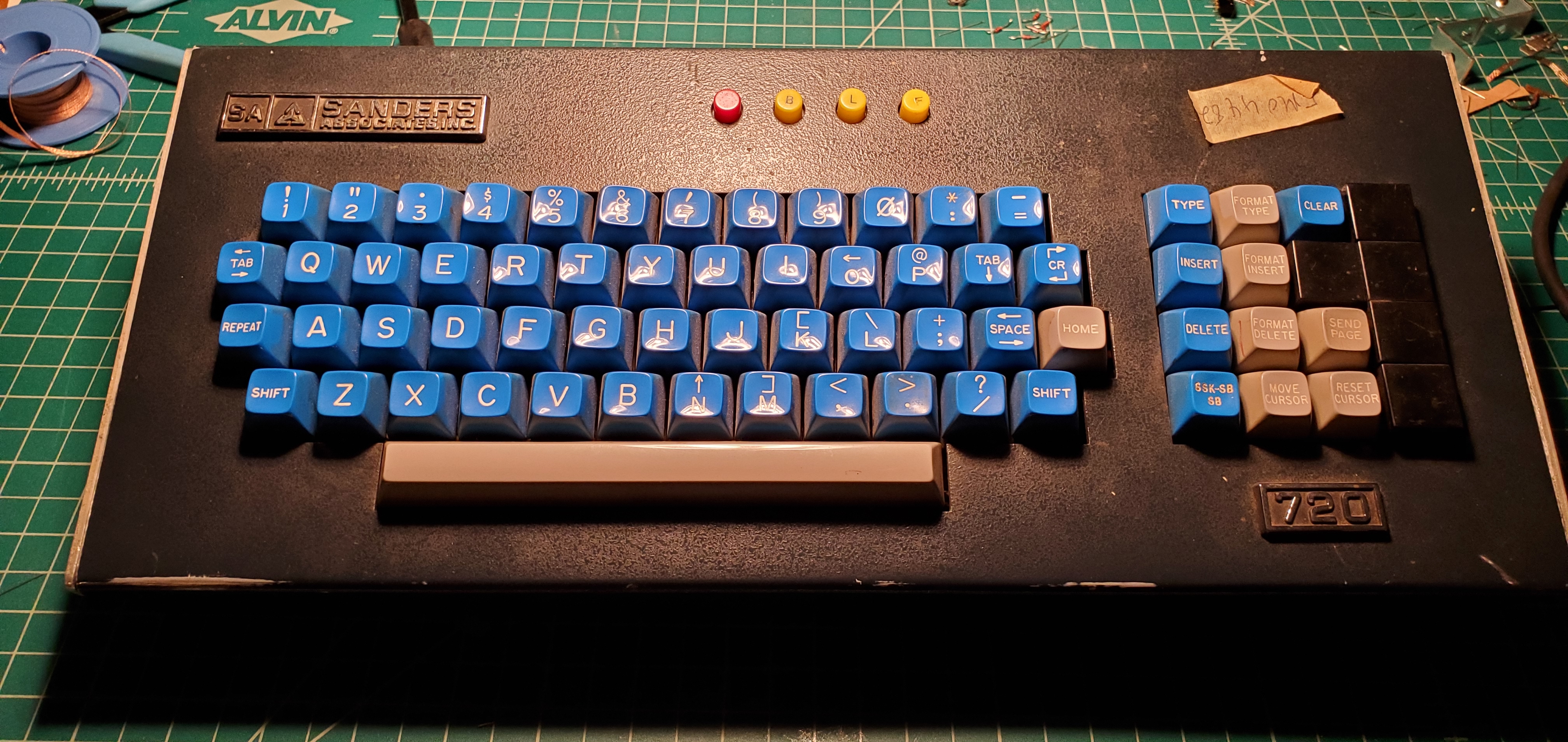
20230428_194920.jpg (3.06 MiB) Viewed 11058 times
20230428_194933.jpg
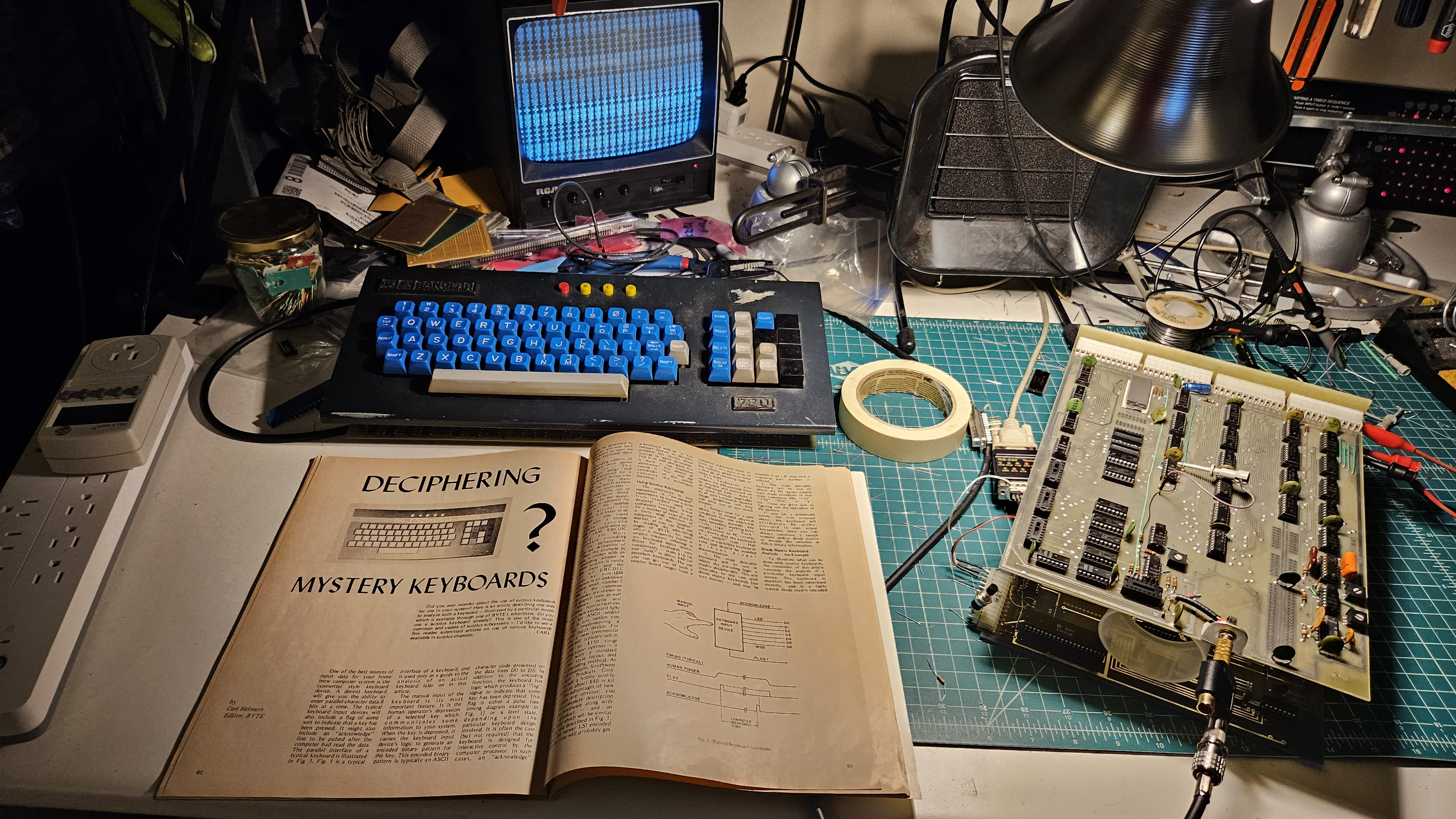
20230428_194933.jpg (2.43 MiB) Viewed 11058 times
20230428_194941.jpg
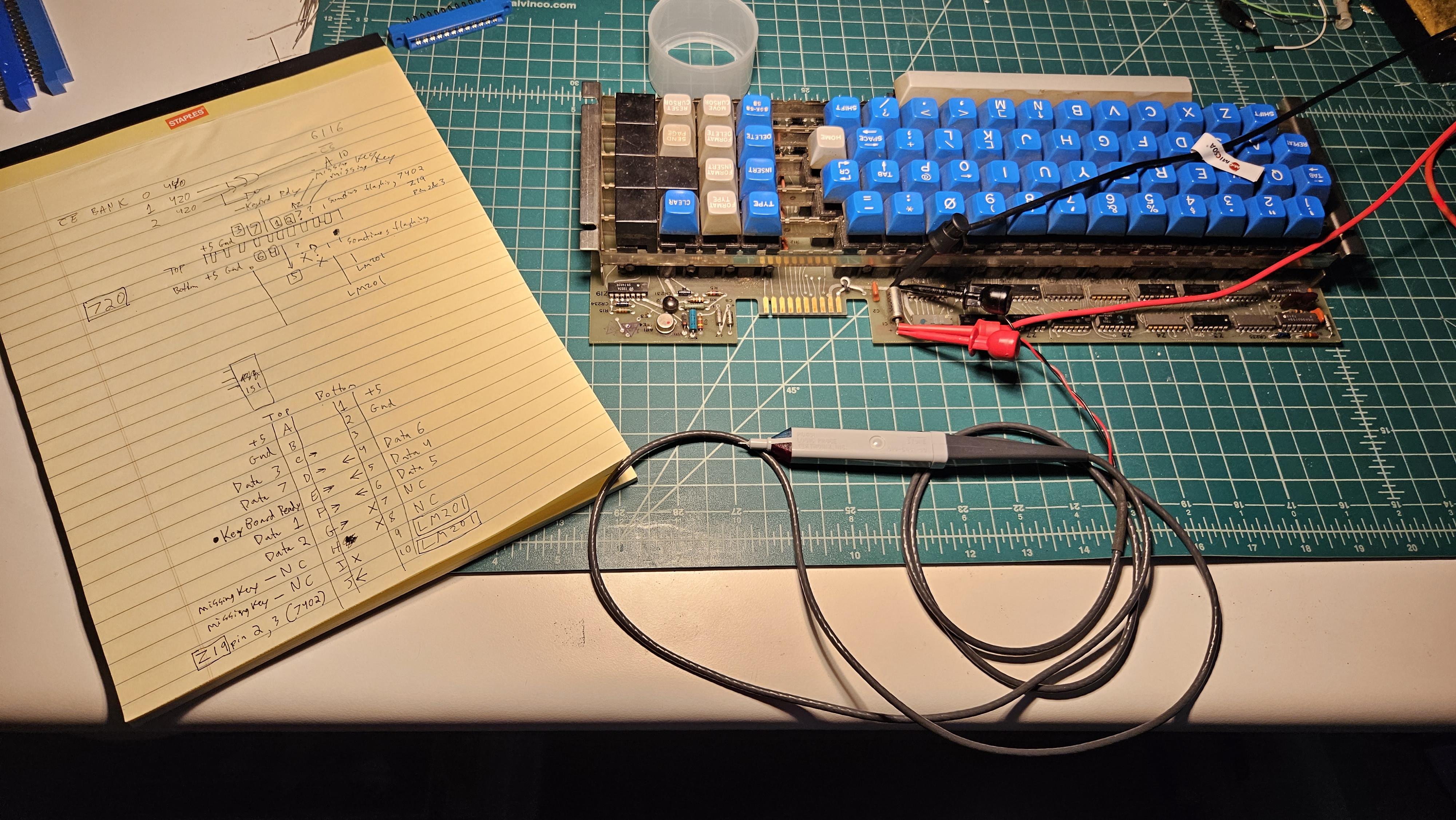
20230428_194941.jpg (2.3 MiB) Viewed 11058 times
Superboard Replica (400, 420C, 440) | C4P (502, 540) | Mini OSI-300 | https://www.commodorez.com 🌵
Mark
Posts: 297
Joined: Tue Sep 16, 2008 6:04 am
Location: Madison, WI
Contact:

Re: Built my 400 replica

Post by Mark »

Hey that's really neat!
I was wondering about the 6512 until I looked up it's specs and realized it's pretty much a pin compatible replacement for 6800. The clock requirements are kind of crazy for those CPUs. Are there pull-ups for the open-collector address buffers somewhere or do they just rely on the passive pullups of the connected chips? Maybe it required resistors on the backplane?
A 144KHz ACIA clock would yield a baudrate of 9000bps. If you can get it to 153600 you'd have 9600bps! (Probably a bit fast for a 1Mhz CPU).

So OSI had support for 6800 in the OSI510 CPU board ROM. It's just 256 bytes and pretty much duplicates the 65A monitor you seem to have in your OSI 400. Although I once disassembled the 6800 binary, it wasn't really in an assemblable state. So I updated it and confirmed it assembles to the same binary found in the OSI ROM. It initializes the ACIA to 8N2 like all older OSI system ROMS as well as enabling IRQs without handlers, so don't connect the 6850 IRQ line.

You will need to make a minor change in that it uses some RAM at $1Fxx for some reason which would not exist on your OSI400 board. It also initializes a memory control PIA at $F700 but it wouldn't matter if it was not present in your system.
You can assemble the code with the A68 cross-assembler updated by Herb Johnson

Code: Select all

                        ; 6800 Disassembly from $FF00 to $FFFF
                        ; 6800 Serial Monitor program for OSI 510 board
                        ; compatible with Herb Johnson's 6800 cross assembler
                        ;
                        ; memory locations used by ROM
   1f34                 L1F34 EQU $1F34
   1f35                 L1F35 EQU $1F35
   1fb0                 L1FB0 EQU $1FB0
   1fdf                 L1FDF EQU $1FDF
   fc00                 ACIA  EQU $FC00
   f700                 PIA   EQU $F700
                        ;
   ff00                 	ORG	$FF00
                        ;
                        ;
   ff00                 LFF00
   ff00   7e ff d3      	JMP	INSER
   ff03   47            	ASRA
   ff04   24 fa         	BCC	LFF00
                        ;
   ff06                 LFF06
   ff06   b6 fc 01      	LDAA	ACIA+1
   ff09   84 7f         	ANDA	#$7F
   ff0b   81 7f         	CMPA	#$7F
   ff0d   27 f1         	BEQ	LFF00
   ff0f   7e ff 88      	JMP	OUTSER
                        
   ff12                 LFF12
   ff12   8d ec         	BSR	LFF00
   ff14   81 52         	CMPA	#$52  ;'R
   ff16   27 13         	BEQ	LFF2B
   ff18   81 30         	CMPA	#$30  ;'0
   ff1a   2b f6         	BMI	LFF12
   ff1c   81 39         	CMPA	#$39  ;'9
   ff1e   2f 0a         	BLE	LFF2A
   ff20   81 41         	CMPA	#$41  ;'A
   ff22   2b ee         	BMI	LFF12
   ff24   81 46         	CMPA	#$46  ;'F
   ff26   2e ea         	BGT	LFF12
   ff28   80 07         	SUBA	#$07
   ff2a   39            LFF2A	RTS
                        
   ff2b   7e ff a8      LFF2B	JMP	LFFA8
                        
   ff2e                 LFF2E
   ff2e   8d 07         	BSR	LFF37
   ff30                 LFF30
   ff30   8d 13         	BSR	LFF45
   ff32   a7 00         	STAA	0, X
   ff34   08            	INX
   ff35   20 f9         	BRA	LFF30
                        
   ff37                 LFF37
   ff37   8d 0c         	BSR	LFF45
   ff39   b7 1f 34      	STAA	L1F34
   ff3c   8d 07         	BSR	LFF45
   ff3e   b7 1f 35      	STAA	L1F35
   ff41   fe 1f 34      	LDX	L1F34
   ff44   39            	RTS
                        
   ff45                 LFF45
   ff45   8d cb         	BSR	LFF12
   ff47   48            	LSLA
   ff48   48            	LSLA
   ff49   48            	LSLA
   ff4a   48            	LSLA
   ff4b   16            	TAB
   ff4c   8d c4         	BSR	LFF12
   ff4e   84 0f         	ANDA	#$0F
   ff50   1b            	ABA
   ff51   39            	RTS
                        
                        
   ff52   00 00         	FCB	$00, $00
                        
   ff54                 LFF54
   ff54   8d e1         	BSR	LFF37
   ff56                 LFF56
   ff56   86 0d         	LDAA	#$0D
   ff58   8d 2e         	BSR	OUTSER
   ff5a   86 0a         	LDAA	#$0A
   ff5c   8d 2a         	BSR	OUTSER
   ff5e   8d 17         	BSR	LFF77
   ff60   8d 15         	BSR	LFF77
   ff62   8d 13         	BSR	LFF77
   ff64   8d 11         	BSR	LFF77
   ff66   8d 0f         	BSR	LFF77
   ff68   8d 0d         	BSR	LFF77
   ff6a   8d 0b         	BSR	LFF77
   ff6c   8d 09         	BSR	LFF77
   ff6e   b6 fc 00      	LDAA	ACIA
   ff71   47            	ASRA
   ff72   24 e2         	BCC	LFF56
   ff74   7e ff b2      	JMP	LFFB2
                        
   ff77                 LFF77
   ff77   8d 26         	BSR	LFF9F
   ff79   39            	RTS
                        
   ff7a                 LFF7A
   ff7a   44            	LSRA
   ff7b   44            	LSRA
   ff7c   44            	LSRA
   ff7d   44            	LSRA
   ff7e                 LFF7E
   ff7e   84 0f         	ANDA	#$0F
   ff80   8b 30         	ADDA	#$30
   ff82   81 39         	CMPA	#$39
   ff84   23 02         	BLS	OUTSER
   ff86   8b 07         	ADDA	#$07
   ff88                 OUTSER
   ff88   37            	PSHB
   ff89                 LFF89
   ff89   f6 fc 00      	LDAB	ACIA
   ff8c   57            	ASRB
   ff8d   57            	ASRB
   ff8e   24 f9         	BCC	LFF89
   ff90   b7 fc 01      	STAA	ACIA+1
   ff93   33            	PULB
   ff94   39            	RTS
                        
   ff95                 LFF95
   ff95   a6 00         	LDAA	0, X
   ff97   8d e1         	BSR	LFF7A
   ff99   a6 00         	LDAA	0, X
   ff9b   8d e1         	BSR	LFF7E
   ff9d   08            	INX
   ff9e   39            	RTS
                        
   ff9f                 LFF9F
   ff9f   8d f4         	BSR	LFF95
   ffa1                 LFFA1
   ffa1   86 20         	LDAA	#$20
   ffa3   20 e3         	BRA	OUTSER
                        
                        
   ffa5   00 00 00      	FCB	$00, $00, $00
                        
   ffa8                 LFFA8
   ffa8   86 03         	LDAA	#$03   ;IRQ, SWI vector entry
   ffaa   b7 fc 00      	STAA	ACIA   ;reset ACIA
   ffad   86 b1         	LDAA	#$B1
   ffaf   b7 fc 00      	STAA	ACIA   ;/16 8N2 +XIRQ +RIRQ
   ffb2                 LFFB2
   ffb2   8e 1f 28      	LDS	#$1F28
   ffb5   86 0d         	LDAA	#$0D
   ffb7   8d cf         	BSR	OUTSER
   ffb9   86 0a         	LDAA	#$0A
   ffbb   8d cb         	BSR	OUTSER
   ffbd   bd ff 00      	JSR	LFF00
   ffc0   16            	TAB
   ffc1   8d de         	BSR	LFFA1
   ffc3   c1 4c         	CMPB	#$4C  ;'L
   ffc5   26 03         	BNE	LFFCA
   ffc7   7e ff 2e      	JMP	LFF2E
                        
   ffca                 LFFCA
   ffca   c1 50         	CMPB	#$50  ;'P
   ffcc   27 86         	BEQ	LFF54
   ffce   c1 47         	CMPB	#$47  ;'G
   ffd0   26 e0         	BNE	LFFB2
   ffd2   3b            	RTI
                        
   ffd3                 INSER
   ffd3   b6 1f df      	LDAA	L1FDF ;$1FDF input redir flag?
   ffd6   27 03         	BEQ	LFFDB
   ffd8   7e 1f b0      	JMP	L1FB0
                        
   ffdb                 LFFDB
   ffdb   b6 fc 00      	LDAA	ACIA  ;Get char from serial
   ffde   47            	ASRA
   ffdf   24 fa         	BCC	LFFDB
   ffe1   7e ff 06      	JMP	LFF06
                        
                        
   ffe4   00 00 00      	FCB	$00, $00, $00
                        
   ffe7                 LFFE7
   ffe7   7f 1f df      	CLR	L1FDF	;reset vector entry
   ffea   c6 00         	LDAB	#$00
   ffec   f7 f7 01      	STAB	PIA+1
   ffef   f7 f7 00      	STAB	PIA  ;Set PIA DDRA to output
   fff2   c6 04         	LDAB	#$04
   fff4   f7 f7 01      	STAB	PIA+1
   fff7   7e ff a8      	JMP	LFFA8
                        ;
                        ;				;IRQ vector ($FFA8)
                        ;FFFA
   fffa   ff a8         	FCB  $FF, $A8  ;SWI instru, int vector ($FFA8)
                        ;FFFC
   fffc   1f e0         	FCB  $1F, $E0  ;NMI vector   ($1FE0)
                        ;FFFE
   fffe   ff e7         	FCB  $FF, $E7  ;reset vector	($FFE7)
                        ;-----------------------------------------------------------------------------
   0000                 	END
fc00  ACIA          ffd3  INSER         1f34  L1F34         1f35  L1F35     
1fb0  L1FB0         1fdf  L1FDF         ff00  LFF00         ff06  LFF06     
ff12  LFF12         ff2a  LFF2A         ff2b  LFF2B         ff2e  LFF2E     
ff30  LFF30         ff37  LFF37         ff45  LFF45         ff54  LFF54     
ff56  LFF56         ff77  LFF77         ff7a  LFF7A         ff7e  LFF7E     
ff89  LFF89         ff95  LFF95         ff9f  LFF9F         ffa1  LFFA1     
ffa8  LFFA8         ffb2  LFFB2         ffca  LFFCA         ffdb  LFFDB     
ffe7  LFFE7         ff88  OUTSER        f700  PIA           
Cheers!
- Mark
Attachments
OSI-6800.zip
OSI510 6800 ROM + ASM
(3.44 KiB) Downloaded 400 times
User avatar
CommodoreZ
Posts: 50
Joined: Wed Oct 17, 2018 11:16 am
Contact:

Re: Built my 400 replica

Post by CommodoreZ »

Mark wrote: Wed May 03, 2023 4:23 pm Are there pull-ups for the open-collector address buffers somewhere or do they just rely on the passive pullups of the connected chips? Maybe it required resistors on the backplane?
Good catch. I wish I had noticed it a few days ago, I had made the mistake of not putting those resistors directly on the PCB, going off of the examples I had seen which lacked then. What I didn't realize is that the examples I was mimicking had those resistors on their backplane. C'est la vie, the order has already been placed with glitchworks for a 582 board. I thought I had one, and it seems I bought connectors to populate one, but I can't seem to find the bare PCB.

I'll see how far I get when the parts arrive in the mail.
Superboard Replica (400, 420C, 440) | C4P (502, 540) | Mini OSI-300 | https://www.commodorez.com 🌵
User avatar
CommodoreZ
Posts: 50
Joined: Wed Oct 17, 2018 11:16 am
Contact:

Re: Built my 400 replica

Post by CommodoreZ »

Success! My 400 is running!

Here's what had to happen:
Attached era-appropriate termination resistors from glitch
Replaced 555 with an era-appropriate TO-99 version, also from glitch (this one is purely cosmetic)
Corrected my wiring mistakes when assembling the TX level shifter
Replaced 74LS04 used to buffer 6850 (damaged part wouldn't pull sufficiently during serial loopback tests)
Jumpered /CTS low on 6850

Lastly, the most frustrating one of all that took some assistance from glitch and tangentdelta on IRC, bypassing VMA output from the 6512. MOS datasheets that I've seen indicate that the 65XX family always outputs a high signal on what was formerly the VMA pin on the 6800, as it is tied to VCC internally. When checking this on my 6512, I saw continuity between VCC and VMA. However, for some reason I was seeing a low signal with occasional spikes which I could not explain. The solution was to disconnect the buffer input that feeds VMA beyond the 6512, and pull the signal high with a resistor. The result is that the logic chain allows the E input on pin 14 of the 6850 to go high when necessary, and output serial data.
20230516_212026.jpg
20230516_212026.jpg (1019.81 KiB) Viewed 10990 times
20230516_212045.jpg
20230516_212045.jpg (1.06 MiB) Viewed 10990 times
I've never used the 65A ROM monitor before, but I guess I need to learn how. I was surprised not to see in the software section of this site, either for a manual or ROM image.

I'm glad my 400 is finally operational.
Superboard Replica (400, 420C, 440) | C4P (502, 540) | Mini OSI-300 | https://www.commodorez.com 🌵
Mark
Posts: 297
Joined: Tue Sep 16, 2008 6:04 am
Location: Madison, WI
Contact:

Re: Built my 400 replica

Post by Mark »

Congratulations on your successes!

You can find OSI's PROM monitor 65V & 65A instructions on my Reference page at https://osi.marks-lab.com/reference/fil ... onitor.pdf or see below.

It is a very limited monitor...

Code: Select all

OSI 65A Serial Monitor Commands
	'R' reset, 
	'P' <address> - dump data as hex from supplied address until keypress encountered
	'L' <address><data> - read hex data from acia until 'R' encountered
	'G' go  
 Upon G command, 65A monitor loads from the following addresses followed by an RTI

 $0129 - Y
 $012A - X
 $012B - A
 $012C - Proc Status  'P'
 $012D - stack pointer 'K'
 $012E - PC Hi
 $012F - PC Lo
 When in Command Mode 65A resets ACIA on every character except L, P, & G
If you create assembler programs for your OSI400, you can assemble them with the A65 macro assembler here which can also directly generate object files in 65A monitor loadable format.
(Also use 8N2 when loading for best results.)

[update] I forgot the 65A ROM image, asm source & instructions are also on my ROMS page as 65A.zip. It can be located at $FE00 to work in conjunction with other OSI boot ROMS, or stand-alone as a single 256 byte ROM image at $FF00
User avatar
CommodoreZ
Posts: 50
Joined: Wed Oct 17, 2018 11:16 am
Contact:

Re: Built my 400 replica

Post by CommodoreZ »

Awesome, thanks Mark!

The OSI65V-440-430 ROM you host on the ROMs page of your site, I'm assuming the 430 referenced in the name is Cassette/Analog I/O board. Is that required to operate the 400 with a 440, or can I omit a 430 from the mix? Also, is BASIC required for a simple test? I'd like to see if my 440 operates, and I've got a small backplane to interconnect the two. Is there anything else I should know before trying to burn a ROM? I lack spare 1702As or any way to burn them, so I intend to make an adapter tower and use a more modern EEPROM to get the job done.

One thing I found amusing is how the Signetics 2513 character generator's datasheet lists +5, -5, and -12 as required voltages. However, the 440 documentation seems to instead reference feeding it -9V instead of -12, just as the 1702A would need on the 400 board. They're undervolting the chip, and using a voltage divider from 2 resistors to cut that in half to feed the -5V, and I'm curious how they determined that they could get away with that.
Superboard Replica (400, 420C, 440) | C4P (502, 540) | Mini OSI-300 | https://www.commodorez.com 🌵
Mark
Posts: 297
Joined: Tue Sep 16, 2008 6:04 am
Location: Madison, WI
Contact:

Re: Built my 400 replica

Post by Mark »

Many of these ROM images were included as unused pages in other ROMS such as the one labeled SYNMON used in C2/C4 cassette and disk systems. Others were found in vintage systems.

It seems the ROM configurations that could be used with OSI440 video systems relied on a connected ASCII keyboard. The OSI65V-440-430.ROM is the monitor ROM used at $FE00 in a system with 8K BASIC and an ASCII keyboard. It supports the S1883 UART and the hooks to make BASIC use it with the cassette I/O on the OSI430 board. Its not designed to be the only ROM in the system the way the 65A ROM is.

If you just want to test your 440 video board, you need nothing more than your serial I/O 400 CPU board. Enter the monitor at type LD0C0 and start typing hex digits to write to the screen. Try LD0A8 48 45 4C 4C 4F 20 57 4F 52 4C 44 21 20 (without spaces)

If you want a single ROM replacement that uses video display with serial keyboard we can work on that.

Attached is a test program that should load with 65A monitor & write a message on your OSI440 screen! You may have to enter a 'G' to invoke it after load.

(Sorry, I don't have any firsthand knowledge about the 2513 ).

-Mark
Attachments
osi440.65a.txt
OSI 65A formatted program
(126 Bytes) Downloaded 395 times
User avatar
CommodoreZ
Posts: 50
Joined: Wed Oct 17, 2018 11:16 am
Contact:

Re: Built my 400 replica

Post by CommodoreZ »

Good news! I got it the 440 running together with the 400.

I was trying it out, testing the video signal, in hopes of getting something on screen, and not having much luck. So I started from the beginning in the schematics and build-up procedures. I calibrated my main clock to 4MHz as precisely as my instruments can determine, and then tried to calibrate the /VS clock to spec. I was having no luck whatsoever, and did not see a viable sync signal that my displays would agree with (I have a myriad of CRTs, some dumber than others, all interconnected in my home video plant).

I was checking signals, discussing timings with TangentDelta, tweaking values, and I came to the conclusion that the timing generated by the 4x 74163's was too short. If I changed the VSYNC timing to fit the suggested range, the counter chain would send a reset signal to the VSYNC 74123 before it could finish, and it would be forever stuck in one state. The solution was to instead increase the master clock speed above the recommended 4MHz to about 4.165MHz (my test equipment needs calibration, so that is an approximation). When I did that, I could dial in the VSYNC to a state that I could tell my displays synced to it, rather than seeing wobbly confusion.

After that, it was a question of "where's the pixel data?" The manual says I should see 24 vertical lines, but I could see nothing. I followed the video mixer, and at TangentDelta's suggestion, I checked to see what was feeding that pixel mixer. I could see alphanumeric blanks from its shift register (upper trace), and valid pulses from T1 (lower trace).
20230523_101538.jpg
20230523_101538.jpg (2.7 MiB) Viewed 10889 times

GS was always high, but T2 was floating. Seems that it was wirewrapped to a pin on the keyboard. Upon T2 being jumpered to ground, I saw lines on screen. Then I reinstalled the 2513, and saw...
20230523_103006.jpg
20230523_103006.jpg (2.52 MiB) Viewed 10889 times
Garbage! Beautiful garbage!


So I added the SRAM back in...
20230523_104119.jpg
20230523_104119.jpg (3.06 MiB) Viewed 10889 times
Different garbage, but I'll take it!

And then I tried the two little snippets you sent me, first generating changes to the text on screen, and then?
20230523_104954.jpg
20230523_104954.jpg (3.77 MiB) Viewed 10889 times
HELLO WORLD!


I think I'm well on my way. I've decided that I should not depopulate my 420c board to provide graphics VRAM for my 440, but instead homebrew something with available parts and keep the 420c intact. Next step will be to try the attached program, but first, sleep.
Once again, I say thank you, Mark!
Superboard Replica (400, 420C, 440) | C4P (502, 540) | Mini OSI-300 | https://www.commodorez.com 🌵
Mark
Posts: 297
Joined: Tue Sep 16, 2008 6:04 am
Location: Madison, WI
Contact:

Re: Built my 400 replica

Post by Mark »

Hey that's great!

Perhaps your build notes could be added to the schematics for any future builders?

I've put together a simple screen handler with some code lifted from the OSIFloppyTest program which receives characters from the OSI400 ACIA and displays them on the screen. Based on your screen shots it should display correctly, although the screen values for left margin, line length & bottom row may need to be tweaked a little bit. It could be expanded with more intelligent character handling, but 1K doesn't leave much room.

Attached is the loadable 65A program the source and its listing.
Good Luck!
Attachments
osi440vid.zip
FC00 ACIA to Screen program
(4.93 KiB) Downloaded 377 times
User avatar
CommodoreZ
Posts: 50
Joined: Wed Oct 17, 2018 11:16 am
Contact:

Re: Built my 400 replica

Post by CommodoreZ »

Thanks for the code, Mark. I'll have to fire up ca65 again, it's been awhile. As for for things I've learned, I think this project (400, 440, etc.) will probably get a page of its own on my website with technical details that will hopefully help others.

When it comes to the 420C RAM board, I've for sure decided to use it as a standard RAM expansion. What I'm not sure about is where to put it in the address space. Do I remove the existing 1K and decoding from my 400, and put the 420 at the bottom of the address space, or do I instead put it on top of the 1K, for a total of 5 contiguous kilobytes? I'm open to suggestions on this matter.

I've shifted over to working on figuring out the Sanders 720 keyboard, and I think I've made some progress. Took some time to follow the traces and verify the pinout to what the 440 documentation says to expect.
Image
Image
Image

I've also discovered a few very important things about the 720 keyboard:
It requires +/-15V to operate an LM201 opamp to do key detection, in what operates like a giant OR gate to trigger the strobe.
It has no CTRL key, and many other expected keys appear to be on different ASCII values, based on what I've seen on the documents I got with it.
The example in Byte is not the exact same as what I have.
While the 720 provides an /ACK input, the 440 doesn't appear to supply that signal at the keyboard port.

I've ordered some power supply options to help me provide the necessary voltages for the 400, 440, and 720, which should be here as early as tomorrow. I've also just received the proper card edge connector to wire internally so I can add in an interposer board to allow me to insert some logic for the missing CTRL key signal. I'd rather not modify the Sanders keyboard irreversibly in the process, and I think I have some ideas on how to do it.

I'm very excited to be making progress on this project. Hopefully in the process I'm doing justice to the 1970s kit computer spirit that is OSI.
Superboard Replica (400, 420C, 440) | C4P (502, 540) | Mini OSI-300 | https://www.commodorez.com 🌵
Post Reply