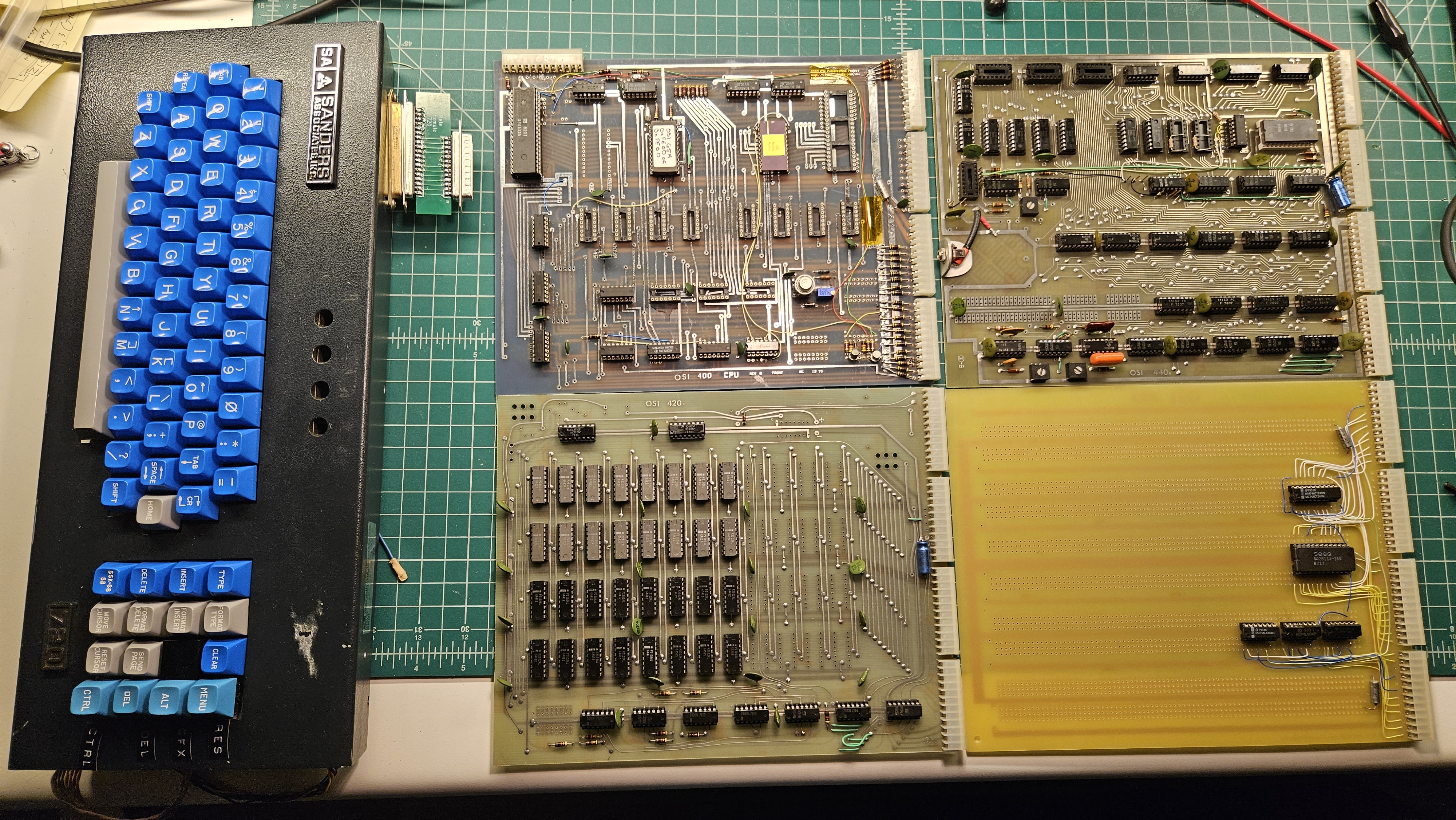
I added a section on my website with some photos of all the 400 build progress of note: https://www.commodorez.com/osi.html
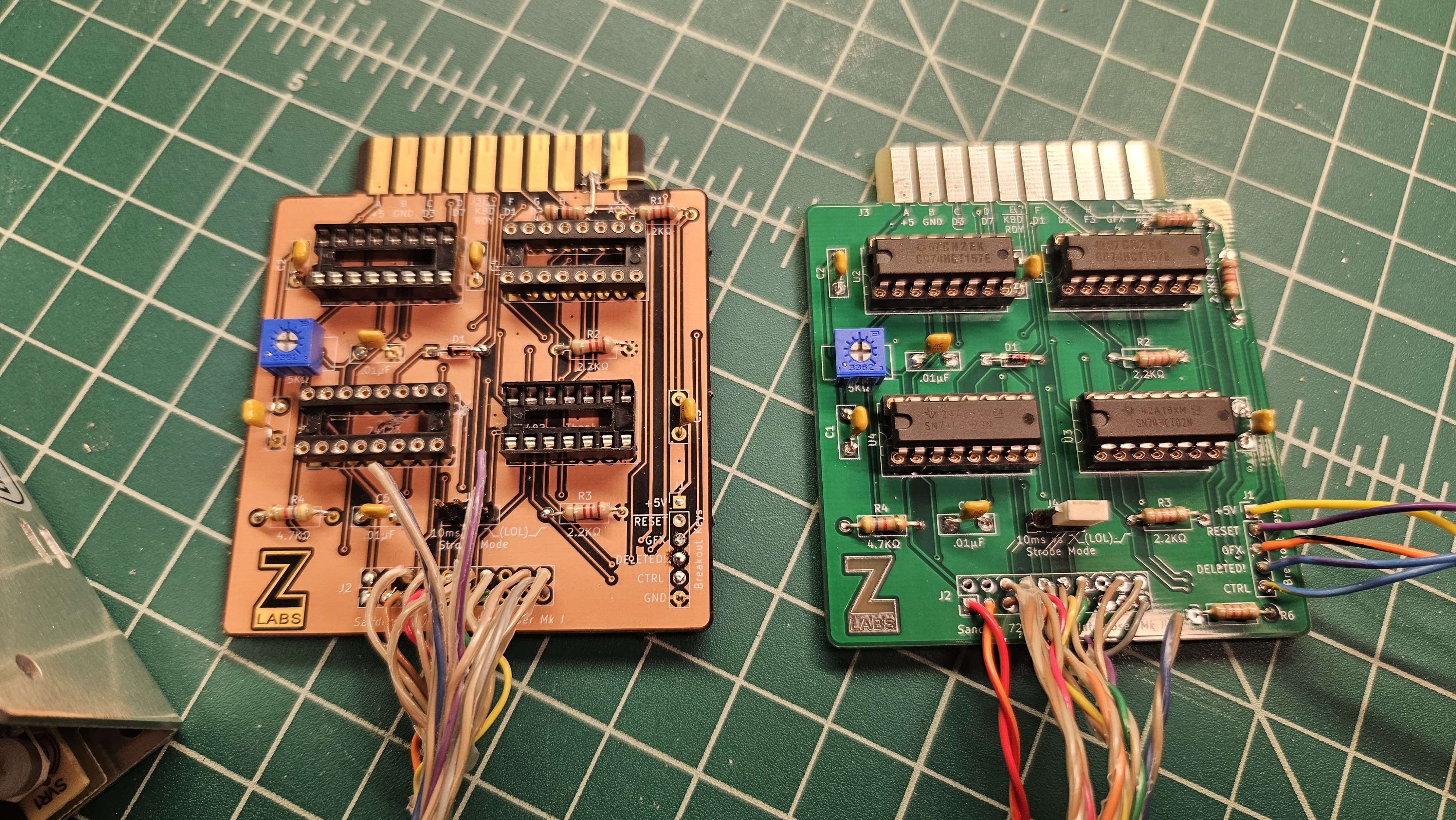
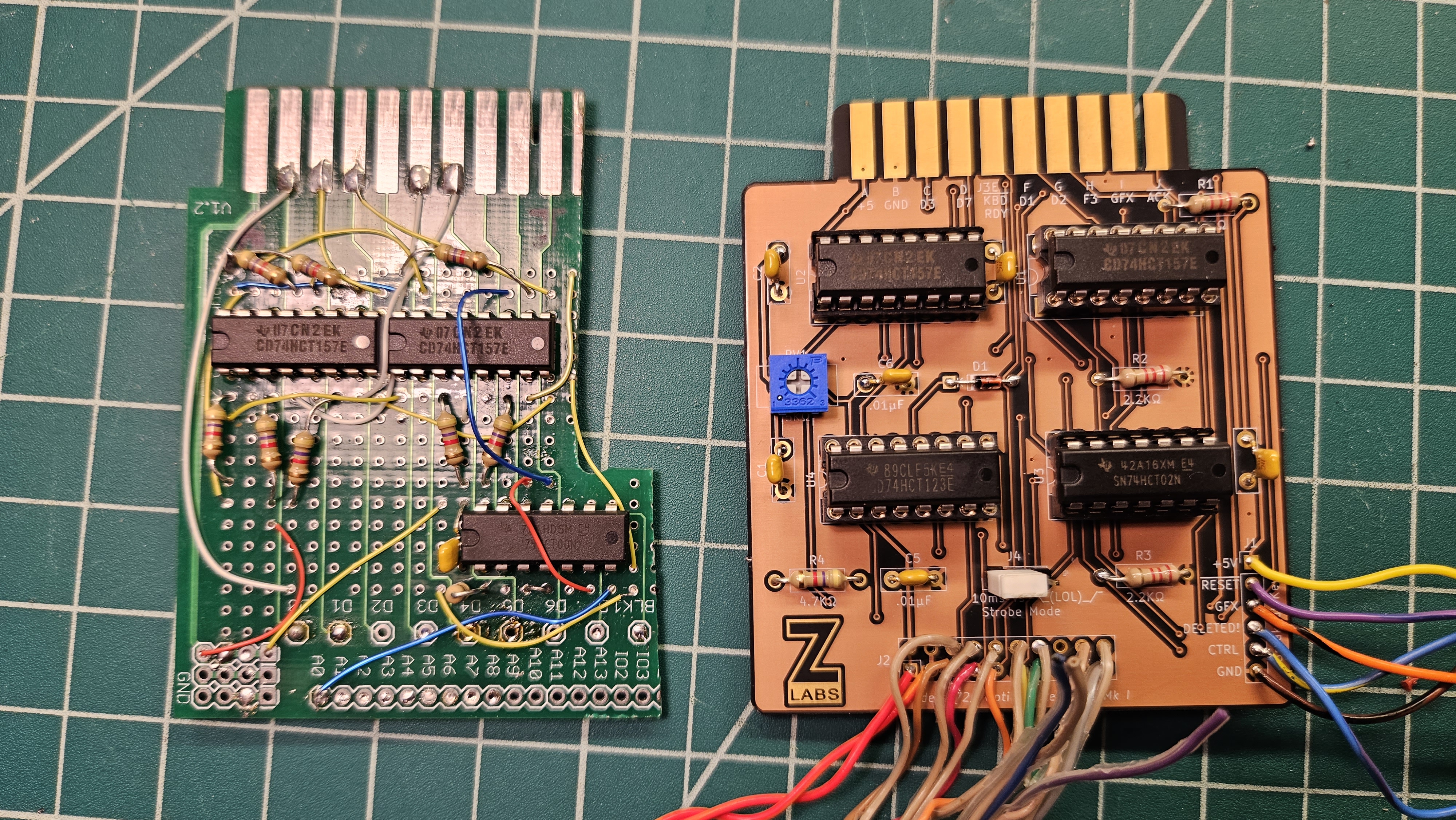
After returning from a trip, I had my new Sanders 720 keyboard interposer PCBs waiting for me. This board's job is to allow me to toggle the 7th data bit as a CTRL key would, as well as add in a proper Delete key (the 720's native Delete sends the wrong ASCII code). I've also given it places for a key to toggle Graphics mode on the 440 using a 7474, and a Reset switch. Initial tests show that I've probably wired up something wrong on both fronts, but that's not surprising considering how many adapters and whatnot are in the mix. I've only spotted one or two design flaws so far. I've also wired one up to a test harness on the bench, and the ASCII responses seem to be okay, but I have yet to do any testing with it plugged into the 440 beyond a power-on test.
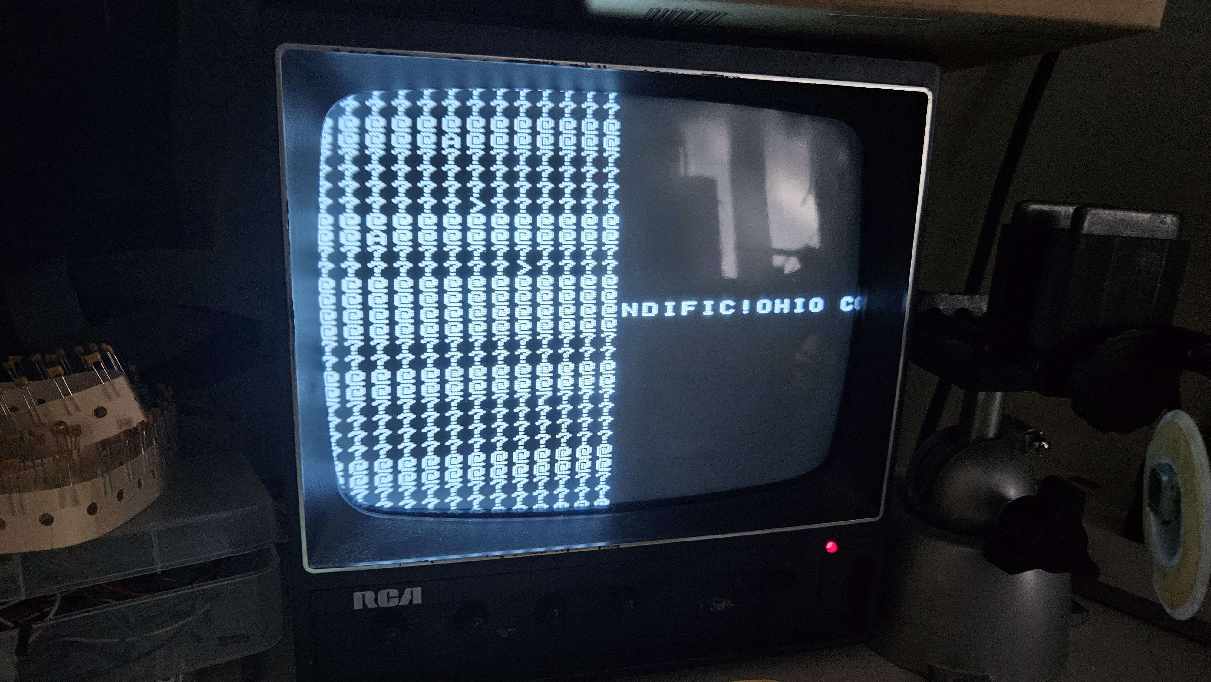
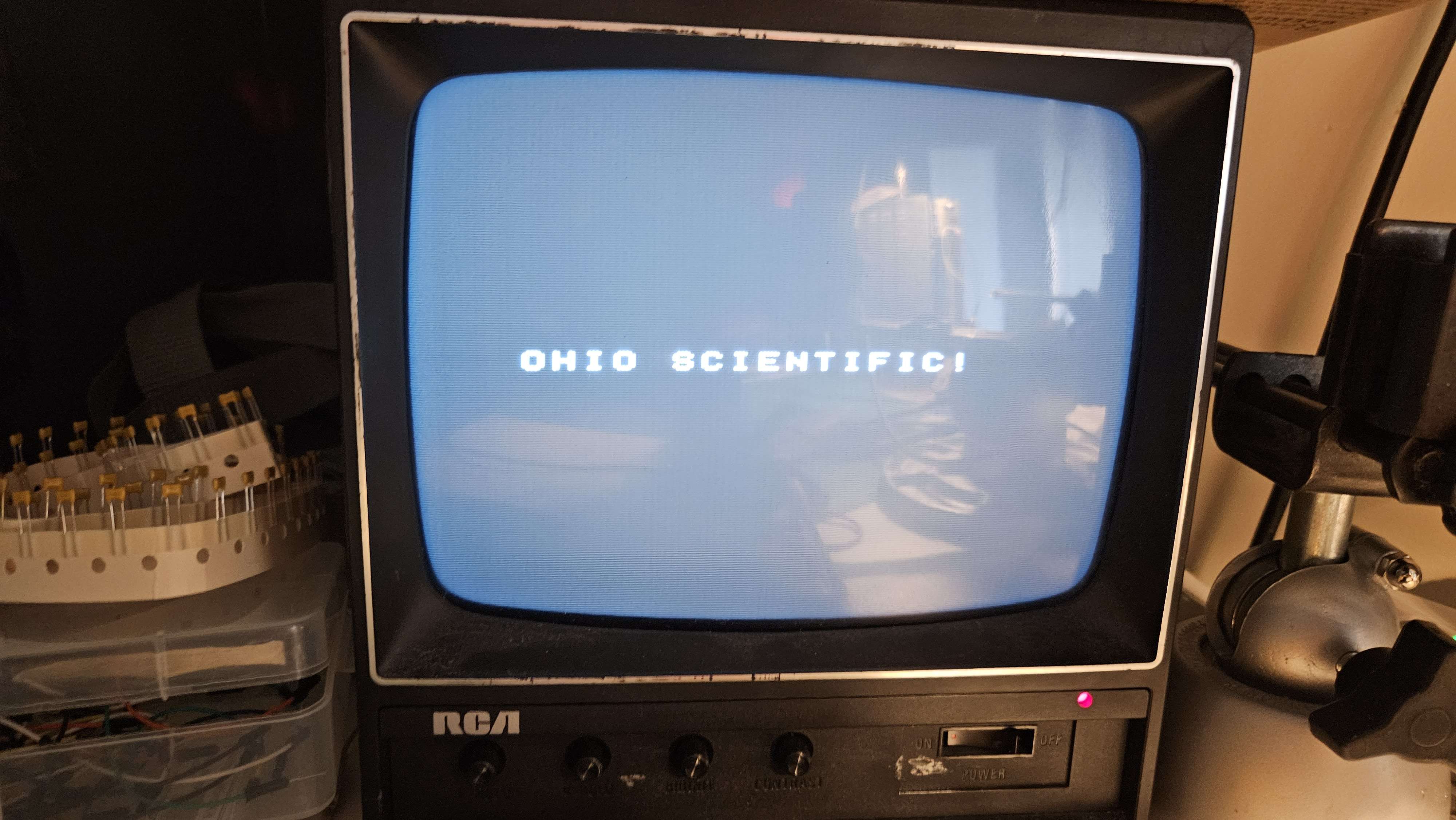
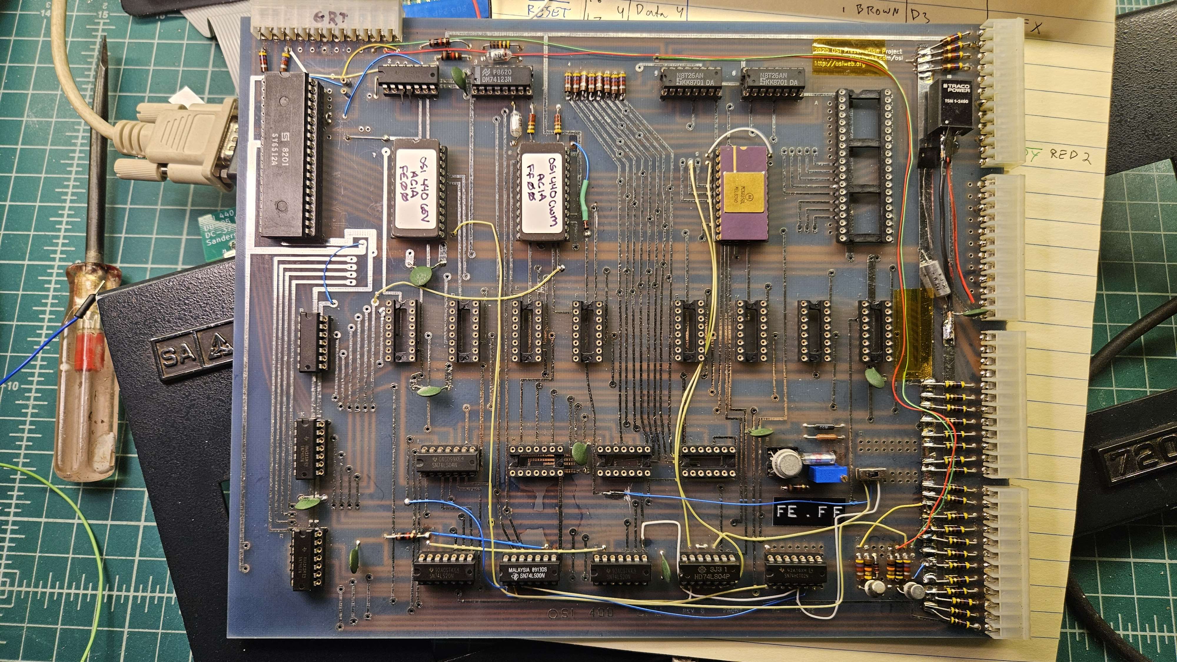
In the meantime, I got frustrated with trying to use what I believe is OS65A (I may be wrong here). I want something I'm more comfortable with to verify the operation of things on the 440, so I elected to assemble the eWoz monitor to a gap in my memory map, $E000, and use a 2816A EEPROM to get it there. Here's the current memory map:
Code: Select all
FE00-FFFF ROM (512B)

FC00-FCFF ACIA (256B)

E400-E7FF Free ROM space
E000-E3FF eWOZ

DC00-DFFF Keyboard (1K, read only)
D400-DBFF Graphics RAM Bank 1 & 2 (2K, 8 bits wide)
D000-D3FF Character RAM (1K, 6 bits wide)

0000-0FFF RAM (4KB)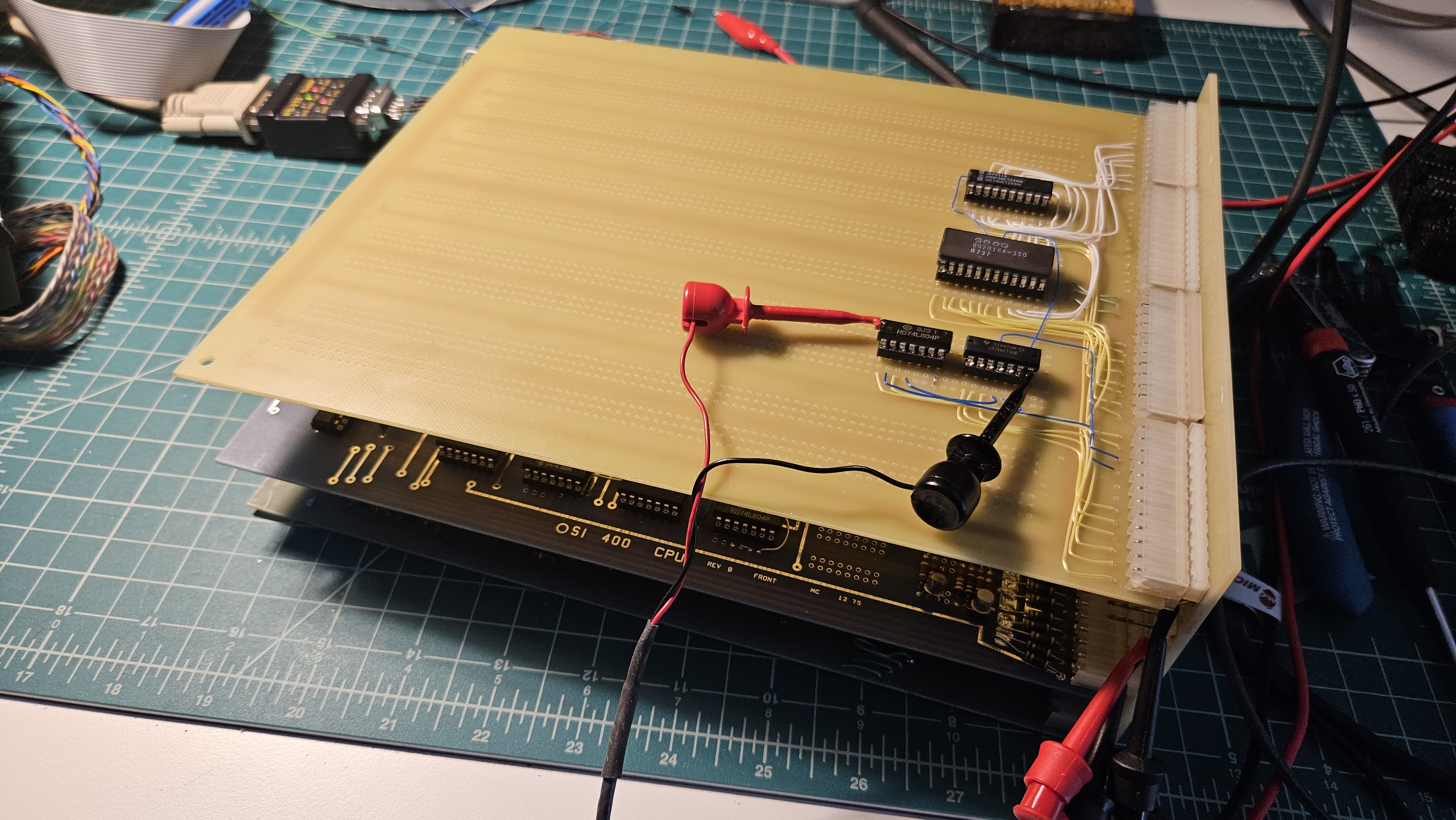
So, a few things to note. My decoupling capacitors are on the underside of the board, but I will probably add more to the top side power rails.
I'm using a 74240 instead of 8T26A's on my 495 protoboard to do data bus buffering and inverting. I've seen glitch have success with these buffers on his massive RAM ROM combo board, and liked the convenience factor.
This photo was taken before I installed a Data Direction diode to talk to the 8T26A's. Initially, I did not understand how that data bus buffer operated, but glitch pointed me in the right direction. It kind of blew my mind to think that each board's diode effectively makes one giant OR gate, each capable of signalling the buffers on the CPU board to allow data to be read. I was able to get data other than $FF from a random MCM2716 using this configuration, but thus far I haven't had any luck with the 2816A that I'd prefer to use for convenience sake. I'm still unable to program 2716's with my current equipment, but I worry that these 2816's are too slow either due to my configuration or the 1MHz bus speed.
Right now, I'm reassessing how I'm doing address decoding as it pertains to /OE and /CE qualification, my 74240 buffer, and triggering the DD signal. I'm thinking that I can get the ROM selected first, ignoring the Phi2 or R/W signals initially while the address is being setup, and then open the proverbial flood gates during when Phi2 and R/W are asserted.
I feel like I'm learning alot here!